Silicon Carbide Wafer Process Platform
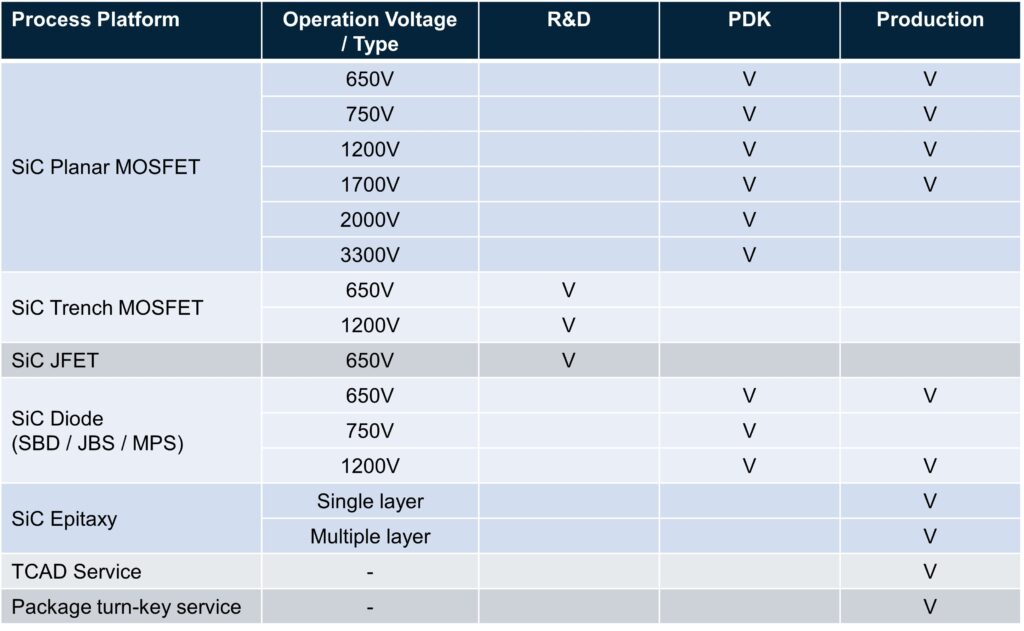
Hon Young Semiconductor offers a comprehensive 6-inch SiC wafer manufacture platform and foundry services, including industrial and automotive Schottky Barrier Diode (SBD) and Power MOSFET technology platforms. The voltage range spans from 650V to 3300V. We are dedicated to provide high-quality, fast, and reliable foundry services, engineering support, quality assurance, and offering the service of the research and development from the third party, establishing ourselves as a trusted long-term partner for our customers.
Customers can leverage Hon Young Semiconductor’s technical support to conduct process and electrical simulations (TCAD Simulation), accelerating product development. We offer SiC epitaxy wafer production, high-temperature implant, high-temperature annealing, film/metal deposition, back-side grinding, back-side metallization, wafer acceptance testing (WAT), and chip probing (CP) services. In addition, we also offer front side metal of Ag, Au, Cu, and Al. We offer turn-key service of packaging and final test (FT).